Amplifier P.A.352 Data
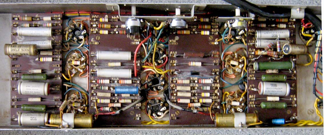
Photograph of amplifier before restoration {large files]
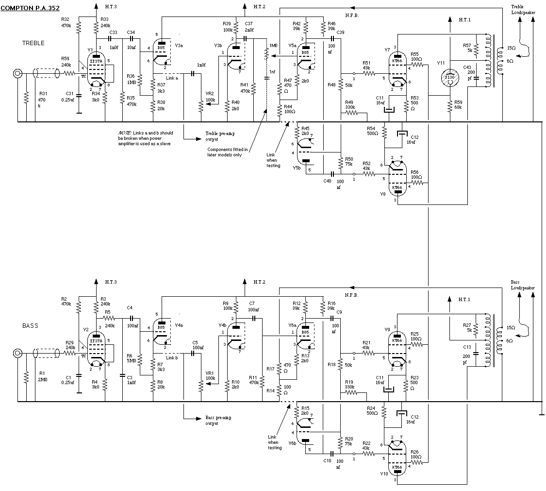
Circuit Diagram
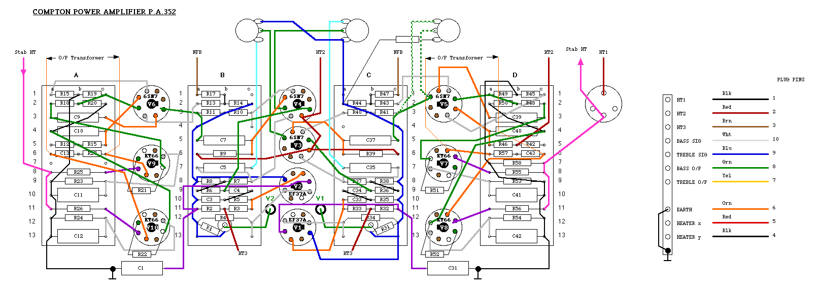
Under Chassis Layout
Colour coding of this diagram: Brown=Neg Feedback . Red=HT . Pink=
Stab HT . Orange=Anode . Magenta=Screened Grid . Green=control grid .
Cyan=other signal wiring . Grey=cathode . Blue=floating signal earth
. Black=chassisearth . Thin black=interconnections. . . Note:
these are not the actual colours used in the amplifier
wiring
Components List RESISTOR
VALUE
FUNCTION
PANEL
LOCATION
1
2M0
V2 grid leak
B
12a
2
470k
V2 SG feed
B
11ab
3
240k
V2 anode load
B
11bc
4
3k0
V2 cathode bias
B
12ac
5
240k
Bass time const
B
10bc
6
5M0
V2 grid leak
B
9ab
7
3k3
V4 cathode bias
B
8bc
8
20k
V4a cathode load
B
8ab
9
100k
V4b anode load
B
6ac
10
2k0
V4b cathode bias
B
3bc
11
470k
V6a grid leak
B
3ab
12
39k
V6a anode load
A
5ab
13
2k0
V6a cathode bias
B
2ab
14
100�
NFB divider bottom
B
2bc
15
2k0
V6b cathode bias
A
1ab
16
39k
V6b anode load
A
5bc
17
470�
NFB divider top
B
1ab
18
50k
Paraphase divider top
A
2ab
19
330k
V9, V10, V6b grid leak
A
1bc
20
75k
Paraphase divider bottom
A
2bc
21
43k
V9 grid stopper
V9 base
22
43k
V10 grid stopper
V10 base
23
500�
V9 cathode bias
A
9ac
24
500�
V10 cathode bias
A
12ac
25
100�
V9 SG feed
A
8ac
26
100�
V10 SG feed
A
11ac
27
5k0
Phase correction
A
6bc
28
29
240k
V2 grid stopper
V2 top cap
30
31
470k
V1 grid leak
C
12c
32
470k
V2 SG feed
C
11bc
33
240k
V2 anode load
C
11ab
34
3k0
V2 cathode bias
C
12ac
35
240k
Treble time const
C
10bc
36
5M0
V2 grid leak
C
9bc
37
3k3
V4 cathode bias
C
9ab
38
20k
V4a cathode load
C
8bc
39
100k
V4b anode load
C
6ac
40
2k0
V4b cathode bias
C
3ab
41
470k
V6a grid leak
C
3bc
42
39k
V6a anode load
D
5bc
43
2k0
V6a cathode bias
C
2bc
44
100�
NFB divider bottom
C
2ab
45
2k0
V6b cathode bias
D
1ab
46
39k
V6b anode load
D
5ab
47
470�
NFB divider top
C
1bc
48
50k
Paraphase divider top
D
2bc
49
330k
V9, V10, V6b grid leak
D
1ab
50
75k
Paraphase divider bottom
D
2ab
51
43k
V7 grid stopper
V7 base
52
43k
V8 grid stopper
V8 base
53
500�
V9 cathode bias
D
9ac
54
500�
V10 cathode bias
D
12ac
55
100�
V9 SG feed
D
8ac
56
100�
V10 SG feed
D
11ac
57
5k0
Phase correction
D
6ab
58
68k
V11 cathode feed
D
7ac
59
240k
V1 grid stopper
V1 top cap
CAPACITOR
VALUE
Min VOLTAGE
FUNCTION
PANEL
LOCATION
1
0.25 uf
500
V2 SG decoupler
B
13a
2
3
1nf
500
Bass time const
B
10ab
4
100 nf
500
Coupling V2-V4a
B
9bc
5
100 nf
100
coupling V4a-VR1
B
7ac
6
7
100 nf
500
Coupling V4b-V6a
B
5ac
8
9
100 nf
500
V6a-V9
A
3ac
10
100 nf
500
V6b-V10
A
4ac
11
100 uf
50
Decoupling V9 cathode
A
10ac
12
100 uf
50
Decoupling V10 cathode
A
13ac
13
200pf
800 AC
Phase correction
A
6ab
31
0.25 uf
500
V1 SG decoupler
C
11c
32
33
1nf
500
Treble time const
C
10ab
34
100 nf
100
Coupling V1-V3a
C
9ab
35
100 nf
500
coupling V3a-VR2
C
7ac
36
37
100 nf
500
Coupling V3b-V5a
C
5ac
38
39
100 nf
500
Coupling V5b-V8
D
3ac
40
100 nf
500
Coupling V5a-V7
D
4ac
41
100 uf
50
Decoupling V7 cathode
D
10ac
42
100 uf
50
Decoupling V8 cathode
D
13ac
43
200 pf
800 AC
Phase correction
D
6bc
Useful source of high voltage capacitors:
T.A.B.
Components
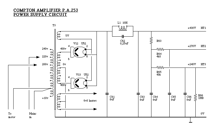
Power Supply Circuit
Power Supply Layout